
BD8316GWL
Aufwärtswandler und invertierter 2-Kanal-DC/DC-Wandler mit eingebautem Leistungs-MOSFET
BD8316GWL
Aufwärtswandler und invertierter 2-Kanal-DC/DC-Wandler mit eingebautem Leistungs-MOSFET
Das BD8316GWL ist ein invertierter Aufwärtsschaltregler mit zwei Kanälen und internem High-Side MOSFET. Mit großem Eingangsbereich von 2,5 bis 5,5 V ist er für den Einsatz tragbarer Bauteile geeignet. Außerdem eignet sich das kompakte Paket ideal für die Miniaturisierung der Stromversorgung.
Für den Automobilbereich kontaktieren Sie bitte unser Sales-Team.
Produktdetails
Spezifikationen:
ch
2
Integrated FET / Controller
Integrated FET
Topology
Boost / Inverting
Synchronous / Nonsynchronous
Non-synchronous
Vin1(Min.)[V]
2.5
Vin1(Max.)[V]
5.5
Vout1(Min.)[V]
2.5
Vout1(Max.)[V]
18
Iout1(Max.)[A]
1
SW frequency setting (Max.)[MHz]
1.76
Operating Temperature (Min.)[°C]
-35
Operating Temperature (Max.)[°C]
85
Package Size [mm]
1.8x1.5 (t=0.55)
Eigenschaften:
・ Wide input voltage range of 2.5V to 5.5 V・ High frequency operation 1.6MHz
・ Incorporates Nch FET of 230mΩ/22V and Pch Pow FET of 230mΩ/15V
・ Incorporates Soft Start (4.2msec(typ))and hight side switch of boost channel
・ Independent ON/OFF signal(STB). Built-in discharge SW for step up channel
・ Small package UCSP50L1( 1.8mm×1.5mm, 4× 3 grid, 11pin, WLCSP)
・ Circuits protection OCP,SCP,UVLO,TSD
Referenzdesign / Anwendungsevaluierungskit
-
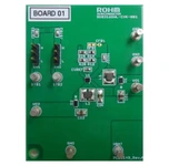
- Evaluation Board - BD8316GWL-EVK-001
The BD8316GWL converter is a power supply solution designed for portable devices. It can operate with a wide input voltage range of 2.5V~5.5V and has a 1μA standby current. It is possible to enable and disable each channel. Users can select which channel to output to, by changing the STB1 and STB2 pins to High or Low. The small package design is suitable for miniaturizing the power supply.
